English
 南非荷兰语
 契维语
 阿姆哈拉语
 阿拉伯语
 阿萨姆语
 艾马拉语
 阿塞拜疆语
 白俄罗斯语
 保加利亚语
 孟加拉语
 波斯尼亚语
 加泰罗尼亚语
 宿务语
 科西嘉语
 捷克语
 威尔士语
 丹麦语
 de
 迪维希语
 希腊语
 英语
 爱沙尼亚语
 波斯语
 芬兰语
 爱尔兰语
 瓜拉尼语
 豪萨语
 希伯来语
 苗语
 克罗地亚语
 海地语
 匈牙利语
 亚美尼亚语
 印尼语
 冰岛语
 意大利语
 日语
 格鲁吉亚语
 高棉语
 韩语
 库尔德语
 吉尔吉斯语
 拉丁语
 卢森堡语
 卢干达语
 林加拉语
 老挝语
 立陶宛语
 拉脱维亚语
 毛利语
 马其顿语
 马来语
 马耳他语
 缅甸语
 尼泊尔语
 荷兰语
 挪威语
 齐切瓦语
 波兰语
 普什图语
 葡萄牙语
 罗马尼亚语
 俄语
 卢旺达语
 信德语
 僧伽罗语
 斯洛伐克语
 斯洛文尼亚语
 萨摩亚语
 索马里语
 阿尔巴尼亚语
 塞尔维亚语
 瑞典语
 斯瓦希里语
 塔吉克语
 泰语
 提格利尼亚语
 土库曼语
 土耳其语
 乌克兰语
 越南语
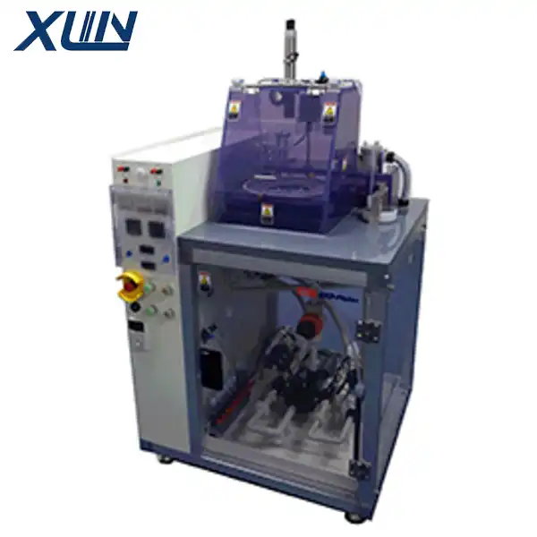
EEJA RAD-Plater Semiconductor Wafer Plating Experimental Equipment
Product Detail
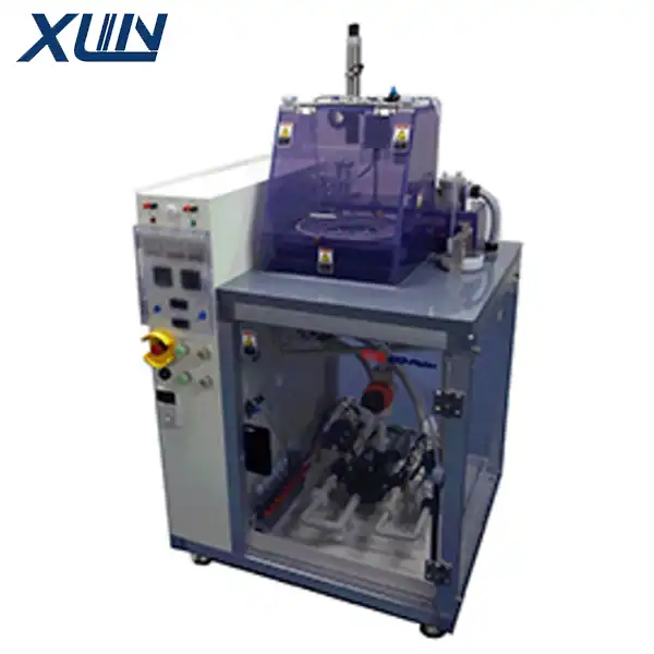 The EEJA RAD-Plater is an ultra-compact, cup-type electroplating system for semiconductor wafers, introduced in 2015 by EEJA, a member of the Tanaka Precious Metals Group. It is designed to enable R&D teams to achieve production-grade electroplating quality in a laboratory setting—at a fraction of the cost of full-scale mass-production equipment.
Core Configuration and Capabilities
Measuring just 800mm in width and 700mm in depth, the unit requires only a standard 100V power supply and compressed air to operate; it is also equipped with casters for easy mobility. It supports wafers ranging from 2 to 8 inches in diameter. The electrolyte volume required is kept under 10 liters—roughly half that of immersion-type systems—which significantly reduces the cost of consumables during experiments. The system is compatible with a wide range of plating chemistries, including gold, silver, palladium, copper, nickel, various alloys, and lead-free solders.
Key Technology: Stir-Cup
The system features EEJA’s proprietary "Stir-Cup" technology. An integrated paddle stirrer enhances the uniformity of the electrolyte across the wafer surface, while a pressure differential mechanism effectively removes air bubbles from within vias (holes). This makes the system exceptionally well-suited for filling high-aspect-ratio vias. Furthermore, by improving ion supply efficiency, the system can achieve a current density of 1.6 A/dm²—significantly higher than the ~0.4 A/dm² typical of conventional laboratory equipment—thereby effectively reducing processing time.
Value Proposition
Priced at approximately one-third to one-quarter of a full-scale production system, the RAD-Plater allows for the replication of production-level plating quality during the R&D phase. This enables the early identification of yield-related issues, preventing defects from surfacing only when the process is scaled up to a mass-production line. The system is primarily targeted at R&D departments within chip manufacturing companies, as well as process development teams at universities and materials suppliers.
Related Products
-
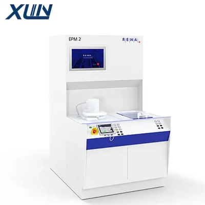
RENA EPM 2 101 F for sale
-
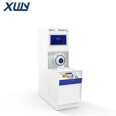
RENA EPM 2 100 F – Manual Electrochemical Deposition (Plating) System
-
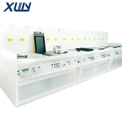
Ramgraber MANUAL PLATER® – electroless for sale
-
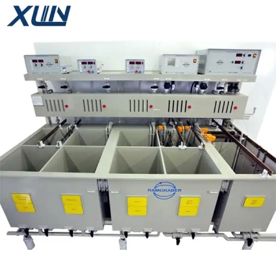
Ramgraber PLATING STAR® Fully Automated Electroplating Production Line
-
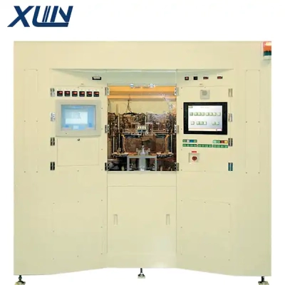
EEJA Cluster Type Fully Automated Cup Electroplating Platform
-
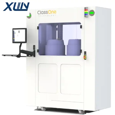
ClassOne Solstice M2 for sale