English
 南非荷兰语
 契维语
 阿姆哈拉语
 阿拉伯语
 阿萨姆语
 艾马拉语
 阿塞拜疆语
 白俄罗斯语
 保加利亚语
 孟加拉语
 波斯尼亚语
 加泰罗尼亚语
 宿务语
 科西嘉语
 捷克语
 威尔士语
 丹麦语
 de
 迪维希语
 希腊语
 英语
 爱沙尼亚语
 波斯语
 芬兰语
 爱尔兰语
 瓜拉尼语
 豪萨语
 希伯来语
 苗语
 克罗地亚语
 海地语
 匈牙利语
 亚美尼亚语
 印尼语
 冰岛语
 意大利语
 日语
 格鲁吉亚语
 高棉语
 韩语
 库尔德语
 吉尔吉斯语
 拉丁语
 卢森堡语
 卢干达语
 林加拉语
 老挝语
 立陶宛语
 拉脱维亚语
 毛利语
 马其顿语
 马来语
 马耳他语
 缅甸语
 尼泊尔语
 荷兰语
 挪威语
 齐切瓦语
 波兰语
 普什图语
 葡萄牙语
 罗马尼亚语
 俄语
 卢旺达语
 信德语
 僧伽罗语
 斯洛伐克语
 斯洛文尼亚语
 萨摩亚语
 索马里语
 阿尔巴尼亚语
 塞尔维亚语
 瑞典语
 斯瓦希里语
 塔吉克语
 泰语
 提格利尼亚语
 土库曼语
 土耳其语
 乌克兰语
 越南语
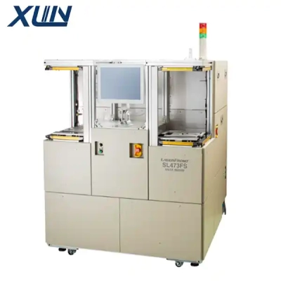
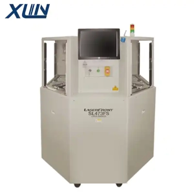
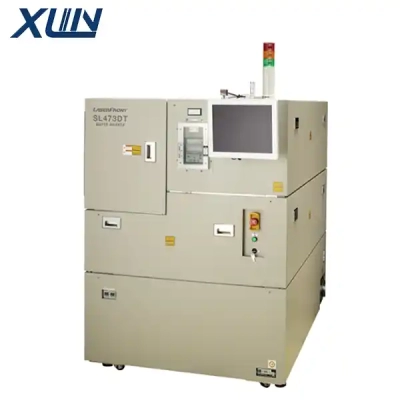
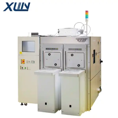
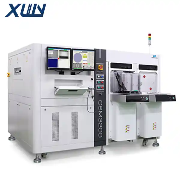
EO Technics CSM3200 Chip-Scale Laser Marking System
Product Detail
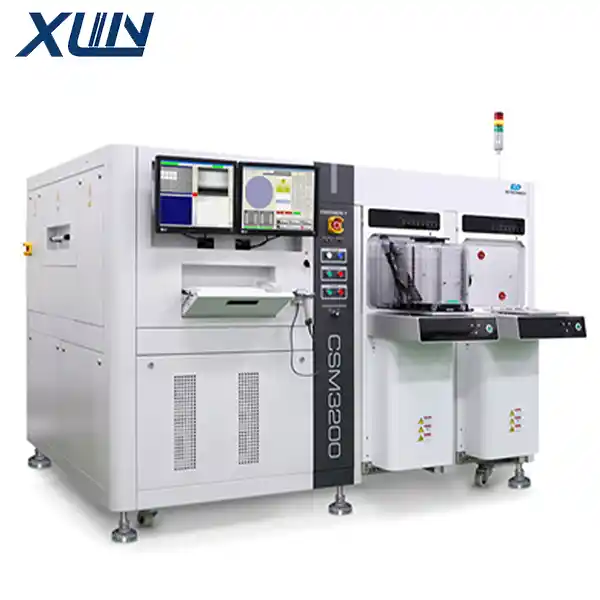 The EO Technics CSM3200 is a laser marking system designed for the backside of wafers. Part of the CSM3200/3300 series, it is specifically engineered for applications such as WLCSP (Wafer-Level Chip-Scale Packaging), enabling non-destructive marking on the wafer backside.
Core Functions
The system features an automatic calibration mechanism that provides real-time compensation for scanner accuracy, ensuring consistent marking positioning. It also integrates an automated inspection function, which verifies marking quality immediately after the process to facilitate closed-loop control.
Key Features
Non-destructive Backside Marking: Designed for wafer-backside processing, it allows for the application of traceability markings without causing damage to the chips.
Versatile Compatibility: The system supports marking requirements for both FFC (Frame-Level Chip) and bare wafer formats, enhancing production line flexibility.
Series Positioning: While it belongs to the same series as the CSM3300, official public documentation does not explicitly detail the specific differences between the two models regarding wafer size capacity or throughput.
Application Scope
This model is primarily used for wafer-level traceability within the semiconductor back-end packaging process—specifically for marking QR codes or characters on the backside of chips in advanced packaging formats like WLCSP. Its design prioritizes self-correcting precision and automated quality verification rather than maximizing marking speed. When selecting equipment, it is recommended to consult the manufacturer to clarify the specific technical distinctions between the CSM3200 and CSM3300, as well as their respective supported wafer sizes.