English
 南非荷兰语
 契维语
 阿姆哈拉语
 阿拉伯语
 阿萨姆语
 艾马拉语
 阿塞拜疆语
 白俄罗斯语
 保加利亚语
 孟加拉语
 波斯尼亚语
 加泰罗尼亚语
 宿务语
 科西嘉语
 捷克语
 威尔士语
 丹麦语
 de
 迪维希语
 希腊语
 英语
 爱沙尼亚语
 波斯语
 芬兰语
 爱尔兰语
 瓜拉尼语
 豪萨语
 希伯来语
 苗语
 克罗地亚语
 海地语
 匈牙利语
 亚美尼亚语
 印尼语
 冰岛语
 意大利语
 日语
 格鲁吉亚语
 高棉语
 韩语
 库尔德语
 吉尔吉斯语
 拉丁语
 卢森堡语
 卢干达语
 林加拉语
 老挝语
 立陶宛语
 拉脱维亚语
 毛利语
 马其顿语
 马来语
 马耳他语
 缅甸语
 尼泊尔语
 荷兰语
 挪威语
 齐切瓦语
 波兰语
 普什图语
 葡萄牙语
 罗马尼亚语
 俄语
 卢旺达语
 信德语
 僧伽罗语
 斯洛伐克语
 斯洛文尼亚语
 萨摩亚语
 索马里语
 阿尔巴尼亚语
 塞尔维亚语
 瑞典语
 斯瓦希里语
 塔吉克语
 泰语
 提格利尼亚语
 土库曼语
 土耳其语
 乌克兰语
 越南语
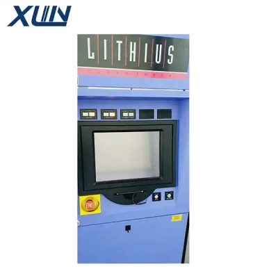
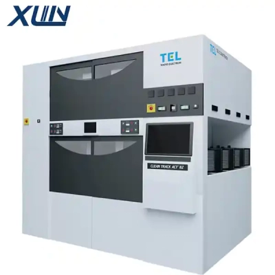
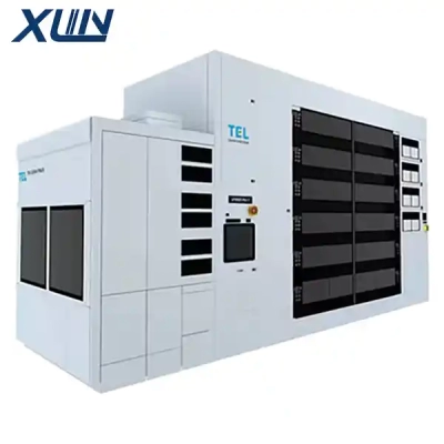
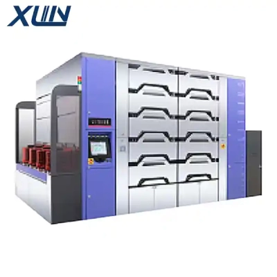
Used TEL Track System MARK Vz
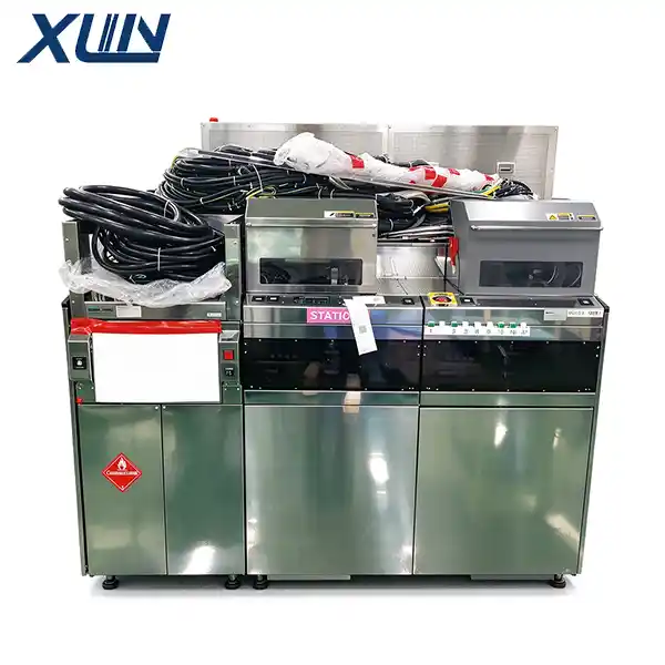
Product Detail
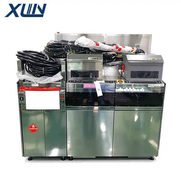 The TEL MARK Vz is a fully automated track system designed for 200mm (8-inch) wafers. As part of Tokyo Electron’s (TEL) classic MARK series, it serves as a highly reliable, high-volume production platform for 8-inch lithography processes.
Core Positioning: A High-Stability, High-Throughput Lithography Hub
This system integrates key lithography-related processes, including photoresist spin-coating, soft baking, post-exposure baking (PEB), developing, and hard baking. It is primarily utilized in production lines for mature-node technologies—such as power semiconductors, analog chips, MEMS, and compound semiconductors—where it ensures process consistency before and after exposure, playing a critical role in maintaining critical dimension (CD) uniformity.
Key Technical Features
Modular Cluster Architecture: The system features a flexible combination of coating, hot plate, cooling, and developing units, supporting parallel processing across multiple chambers. A central robotic handler facilitates high-speed wafer transport, which can be optimized based on production line takt time to achieve high throughput and high equipment utilization.
Precision Thermal and Fluid Management: Multi-zone, independently controlled hot plates ensure uniform baking and minimize pattern distortion. The coating and developing units incorporate precise control over spin speed and chemical flow rates, guaranteeing uniform photoresist thickness and stable development processes.
High-Cleanliness Automated Integration: The system includes an integrated "mini-environment" to prevent particle contamination. It supports automated wafer-carrier loading/unloading and SECS/GEM communication, allowing for seamless integration with various stepper/scanner lithography tools within fully automated production lines.
Summary
With its mature coating and developing processes, flexible modular configuration, and exceptional automation capabilities, the MARK Vz serves as an essential piece of equipment for ensuring lithography yield and production efficiency in 200mm mature-node and specialty-process manufacturing lines.