English
 南非荷兰语
 契维语
 阿姆哈拉语
 阿拉伯语
 阿萨姆语
 艾马拉语
 阿塞拜疆语
 白俄罗斯语
 保加利亚语
 孟加拉语
 波斯尼亚语
 加泰罗尼亚语
 宿务语
 科西嘉语
 捷克语
 威尔士语
 丹麦语
 de
 迪维希语
 希腊语
 英语
 爱沙尼亚语
 波斯语
 芬兰语
 爱尔兰语
 瓜拉尼语
 豪萨语
 希伯来语
 苗语
 克罗地亚语
 海地语
 匈牙利语
 亚美尼亚语
 印尼语
 冰岛语
 意大利语
 日语
 格鲁吉亚语
 高棉语
 韩语
 库尔德语
 吉尔吉斯语
 拉丁语
 卢森堡语
 卢干达语
 林加拉语
 老挝语
 立陶宛语
 拉脱维亚语
 毛利语
 马其顿语
 马来语
 马耳他语
 缅甸语
 尼泊尔语
 荷兰语
 挪威语
 齐切瓦语
 波兰语
 普什图语
 葡萄牙语
 罗马尼亚语
 俄语
 卢旺达语
 信德语
 僧伽罗语
 斯洛伐克语
 斯洛文尼亚语
 萨摩亚语
 索马里语
 阿尔巴尼亚语
 塞尔维亚语
 瑞典语
 斯瓦希里语
 塔吉克语
 泰语
 提格利尼亚语
 土库曼语
 土耳其语
 乌克兰语
 越南语
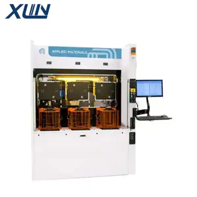
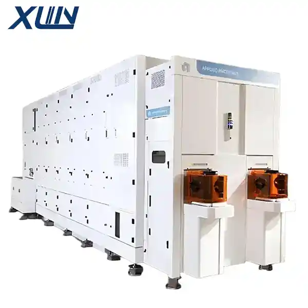
Used Applied Materials Semiconductor Electroplating System Nokota™ ECD
Product Detail
 The Nokota™ ECD is a 300mm wafer-level electrochemical deposition (electroplating) system from Applied Materials. Part of the company’s electroplating product line, it primarily serves advanced packaging and back-end-of-line (BEOL) copper interconnect applications, while also covering certain front-end-of-line (FEOL) copper interconnect processes.
Process Focus: The system utilizes electroplating to deposit metal layers—most notably copper. Typical applications include under-bump metallization (UBM), copper pillars, redistribution layers (RDL), through-silicon via (TSV) filling, and copper interconnects for wafer-level packaging. It addresses challenges such as achieving uniform film thickness for micron-scale metal interconnects and ensuring defect-free filling of high-aspect-ratio structures—a distinct process category from the atomic-level precision offered by ALD/CVD technologies used in front-end manufacturing.
Design Priorities: The Nokota ECD emphasizes film thickness uniformity, high-quality filling, and repeatability for high-volume manufacturing. It features precision plating cells and advanced flow-field control, with optimizations specifically designed to mitigate wafer-edge effects. The system supports automated wafer handling and recipe management, meeting the throughput and stability requirements of high-volume production lines. Its platform architecture allows for flexible switching between various packaging-related plating recipes, enabling production lines to accommodate a diverse range of packaging requirements.
Market Positioning: The Nokota competes in the advanced packaging electroplating space alongside systems like the RAIDER Edge ECD and the ASMPT Stratus P300/P500; it is classified as electroplating equipment rather than a general thin-film deposition tool. Within the broader process chain, it complements Applied Materials’ own front-end deposition equipment, establishing a workflow that spans from front-end film formation to back-end electroplated interconnects.
In short, the Nokota ECD is one of Applied Materials’ primary high-volume production platforms for 300mm wafer-level packaging electroplating.