English
 南非荷兰语
 契维语
 阿姆哈拉语
 阿拉伯语
 阿萨姆语
 艾马拉语
 阿塞拜疆语
 白俄罗斯语
 保加利亚语
 孟加拉语
 波斯尼亚语
 加泰罗尼亚语
 宿务语
 科西嘉语
 捷克语
 威尔士语
 丹麦语
 de
 迪维希语
 希腊语
 英语
 爱沙尼亚语
 波斯语
 芬兰语
 爱尔兰语
 瓜拉尼语
 豪萨语
 希伯来语
 苗语
 克罗地亚语
 海地语
 匈牙利语
 亚美尼亚语
 印尼语
 冰岛语
 意大利语
 日语
 格鲁吉亚语
 高棉语
 韩语
 库尔德语
 吉尔吉斯语
 拉丁语
 卢森堡语
 卢干达语
 林加拉语
 老挝语
 立陶宛语
 拉脱维亚语
 毛利语
 马其顿语
 马来语
 马耳他语
 缅甸语
 尼泊尔语
 荷兰语
 挪威语
 齐切瓦语
 波兰语
 普什图语
 葡萄牙语
 罗马尼亚语
 俄语
 卢旺达语
 信德语
 僧伽罗语
 斯洛伐克语
 斯洛文尼亚语
 萨摩亚语
 索马里语
 阿尔巴尼亚语
 塞尔维亚语
 瑞典语
 斯瓦希里语
 塔吉克语
 泰语
 提格利尼亚语
 土库曼语
 土耳其语
 乌克兰语
 越南语
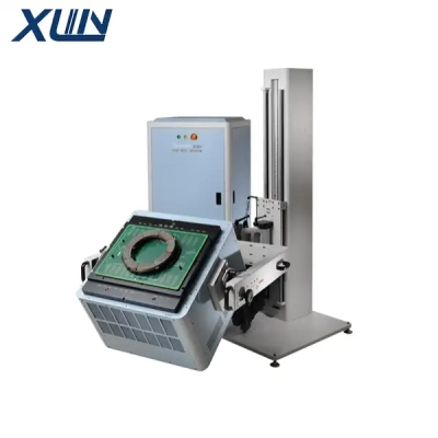
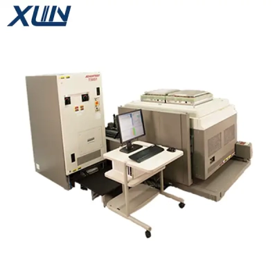
Used Advantest T5833

Product Detail
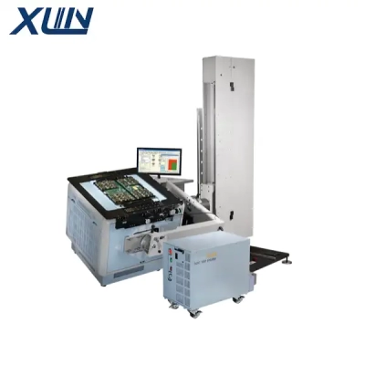
 The T5833 is a cost-effective, high-volume memory test system introduced by Advantest in 2015. Unlike the T5830 (focused on flash memory cost) and the T5503HS2 (designed for high-speed DRAM)—both of which you previously inquired about—the T5833’s core strategy is to cover both DRAM and NAND flash—across both wafer-level and final package-level testing—on a single platform, emphasizing versatility and low testing costs.
Parallelism: It supports the simultaneous testing of 2,048 devices during wafer-level testing (in a 2 I/O configuration) and 512 devices during final package-level testing (in an 8 I/O configuration). It offers test speeds of up to 2.4 Gbps with an overall timing accuracy of ±75ps. It supports LPDDR3 DRAM, high-speed NAND, and next-generation non-volatile memory (NVM) technologies such as MRAM, RRAM, and PCM.
Key Architecture: The system utilizes a "Tester-per-Site" architecture, where each test site features an independent processor to optimize the test flow. It includes built-in high-speed failure address storage and Memory Redundancy Analysis (MRA) capabilities—features that Advantest notes are critical for reducing wafer-level test times and improving yields.
Platform Scalability: Built on Advantest’s AS modular platform, the system can scale from engineering validation configurations to high-volume production, with modular upgrades available to accommodate future device generations. It runs on the FutureSuite operating system and is compatible with test programs developed for the T58xx series.
In short, the T5833 is a general-purpose platform that Advantest introduced during the boom in mobile memory. By enabling a "single-system" approach—covering both DRAM and NAND, as well as both wafer and package testing—it helps drive down overall testing costs. It serves as a complement to the more specialized T5830 and T5503HS2 systems you asked about earlier.