English
 南非荷兰语
 契维语
 阿姆哈拉语
 阿拉伯语
 阿萨姆语
 艾马拉语
 阿塞拜疆语
 白俄罗斯语
 保加利亚语
 孟加拉语
 波斯尼亚语
 加泰罗尼亚语
 宿务语
 科西嘉语
 捷克语
 威尔士语
 丹麦语
 de
 迪维希语
 希腊语
 英语
 爱沙尼亚语
 波斯语
 芬兰语
 爱尔兰语
 瓜拉尼语
 豪萨语
 希伯来语
 苗语
 克罗地亚语
 海地语
 匈牙利语
 亚美尼亚语
 印尼语
 冰岛语
 意大利语
 日语
 格鲁吉亚语
 高棉语
 韩语
 库尔德语
 吉尔吉斯语
 拉丁语
 卢森堡语
 卢干达语
 林加拉语
 老挝语
 立陶宛语
 拉脱维亚语
 毛利语
 马其顿语
 马来语
 马耳他语
 缅甸语
 尼泊尔语
 荷兰语
 挪威语
 齐切瓦语
 波兰语
 普什图语
 葡萄牙语
 罗马尼亚语
 俄语
 卢旺达语
 信德语
 僧伽罗语
 斯洛伐克语
 斯洛文尼亚语
 萨摩亚语
 索马里语
 阿尔巴尼亚语
 塞尔维亚语
 瑞典语
 斯瓦希里语
 塔吉克语
 泰语
 提格利尼亚语
 土库曼语
 土耳其语
 乌克兰语
 越南语
Applied Materials VeritySEM 6D CD-SEM for sale
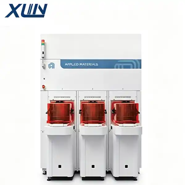
Product Detail
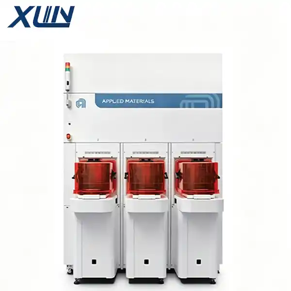 The VeritySEM 6D is a critical dimension scanning electron microscope (CD-SEM) from Applied Materials, specifically designed for high-volume manufacturing metrology of dielectric materials and compound semiconductors. It offers superior process control capabilities compared to conventional silicon-based solutions.
Core Positioning
As a derivative of the widely adopted VeritySEM 6i system, the 6D model is engineered for dielectric materials—such as glass and sapphire—as well as compound semiconductors (e.g., SiC, GaN) and traditional silicon wafers. It is specifically adapted to address the unique challenges posed by dielectric materials, which are prone to charging during manufacturing and exhibit significant variations in dimensions, thickness, and conductivity.
Key Capabilities
Broad Wafer Compatibility: The automated wafer-handling system is self-adjusting, supporting 6-inch, 8-inch, and 12-inch wafers, while accommodating varying thicknesses and levels of wafer warpage.
High-Precision 3D and HAR Metrology: Its high-precision specifications enable the measurement of advanced 3D structures and high-aspect-ratio (HAR) patterns, such as those found in the vertical transistors used in power devices.
High Throughput and Automation: Exceptional imaging resolution and inspection efficiency maximize throughput, while advanced automation and tool-matching precision virtually eliminate the need for manual intervention.
In short, the VeritySEM 6D is a specialized CD-SEM model tailored for non-silicon materials and dielectric substrates. It fills a critical gap left by standard silicon-based CD-SEMs, providing the targeted wafer-handling and metrology capabilities required for compound semiconductor and glass-substrate applications.
Related Products
-
Used Applied Materials VeritySEM 6C CD-SEM
-
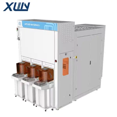
Applied Materials VeritySEM AP E-beam CD Metrology System
-
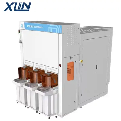
Applied Materials VeritySEM 20 CD-SEM for sale
-
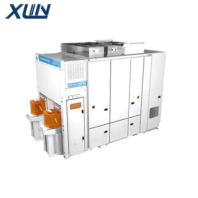
Applied Materials Vera Brightfield Patterned Wafer Optical Inspection System
-
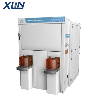
Used Applied Materials SEMVision H20
-
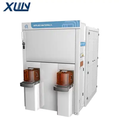
Applied Materials SEMVision G10 CFE Electron-Beam Defect Review and Analysis System