English
 南非荷兰语
 契维语
 阿姆哈拉语
 阿拉伯语
 阿萨姆语
 艾马拉语
 阿塞拜疆语
 白俄罗斯语
 保加利亚语
 孟加拉语
 波斯尼亚语
 加泰罗尼亚语
 宿务语
 科西嘉语
 捷克语
 威尔士语
 丹麦语
 de
 迪维希语
 希腊语
 英语
 爱沙尼亚语
 波斯语
 芬兰语
 爱尔兰语
 瓜拉尼语
 豪萨语
 希伯来语
 苗语
 克罗地亚语
 海地语
 匈牙利语
 亚美尼亚语
 印尼语
 冰岛语
 意大利语
 日语
 格鲁吉亚语
 高棉语
 韩语
 库尔德语
 吉尔吉斯语
 拉丁语
 卢森堡语
 卢干达语
 林加拉语
 老挝语
 立陶宛语
 拉脱维亚语
 毛利语
 马其顿语
 马来语
 马耳他语
 缅甸语
 尼泊尔语
 荷兰语
 挪威语
 齐切瓦语
 波兰语
 普什图语
 葡萄牙语
 罗马尼亚语
 俄语
 卢旺达语
 信德语
 僧伽罗语
 斯洛伐克语
 斯洛文尼亚语
 萨摩亚语
 索马里语
 阿尔巴尼亚语
 塞尔维亚语
 瑞典语
 斯瓦希里语
 塔吉克语
 泰语
 提格利尼亚语
 土库曼语
 土耳其语
 乌克兰语
 越南语
Used SEMES LOUTS
Product Detail
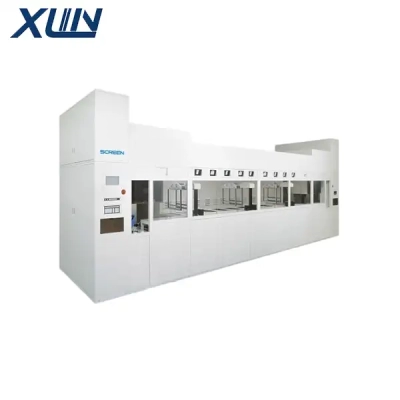
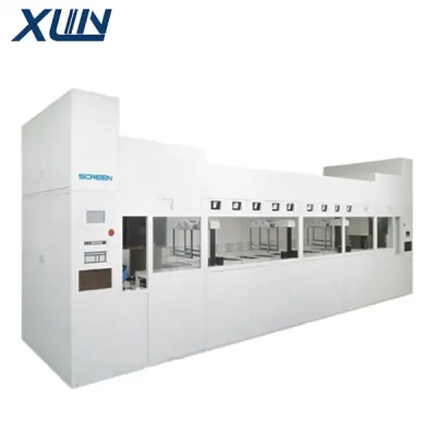
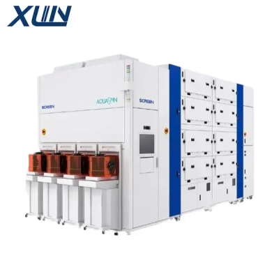
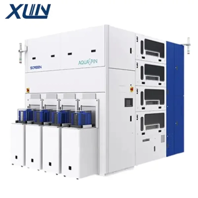
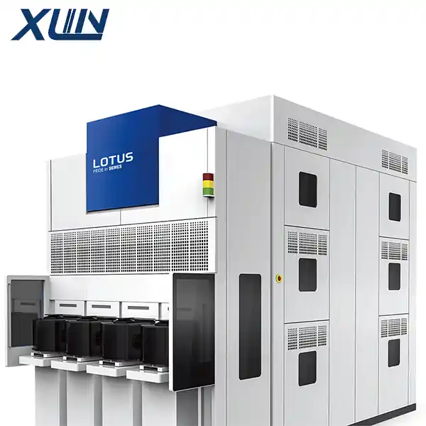
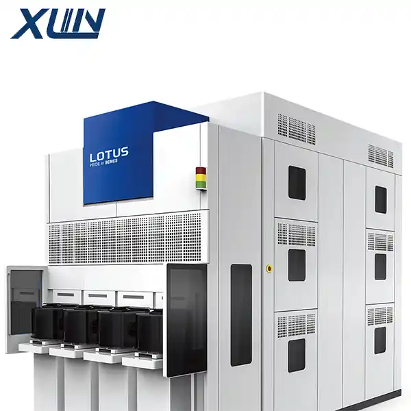 SEMES LOUTS is a single-wafer wet processing system designed for 300mm wafers. Its name is derived from "Lotus," symbolizing the achievement of exceptional cleanliness and surface purity within a liquid environment; it is primarily utilized for precision cleaning and surface treatment in advanced semiconductor manufacturing processes.
Core Positioning: High-Cleanliness Single-Wafer Processing
The LOUTS system employs a single-wafer, rotating-substrate architecture. Wafers are held on a chuck and subjected to a sequential process of chemical dispensing, deionized water rinsing, and drying. This single-wafer approach eliminates the risk of cross-contamination—a common drawback of batch (tank-based) cleaning—and allows for millisecond-level precision in controlling chemical reaction times, meeting the stringent, ultra-low defect rate requirements of advanced process nodes.
Key Technical Features
Optimized Chamber Fluid Dynamics: The internal chamber is precision-engineered to manage airflow patterns and drainage paths. Combined with a sophisticated drying process, this effectively prevents the formation of watermarks and the re-adhesion of particles, ensuring superior surface cleanliness.
Flexible Chemical Compatibility: The system supports the precise mixing and delivery of various chemicals—such as SC1, diluted HF, and O₃-infused water—making it adaptable to a wide range of applications, including post-CMP cleaning, post-etch cleaning, and pre-bonding surface preparation.
Fully Automated Integration: Equipped with standard FOUP loading/unloading capabilities and SECS/GEM communication protocols, the system offers high throughput and integrates seamlessly into fully automated 300mm high-volume production lines.
Summary
Through refined fluid control and high operational stability, the LOUTS system provides a single-wafer wet processing solution for 300mm production lines that balances exceptional cleanliness with high productivity. It serves as a critical tool for ensuring high yields in the manufacturing of advanced logic and memory devices, as well as in semiconductor packaging processes.