English
 南非荷兰语
 契维语
 阿姆哈拉语
 阿拉伯语
 阿萨姆语
 艾马拉语
 阿塞拜疆语
 白俄罗斯语
 保加利亚语
 孟加拉语
 波斯尼亚语
 加泰罗尼亚语
 宿务语
 科西嘉语
 捷克语
 威尔士语
 丹麦语
 de
 迪维希语
 希腊语
 英语
 爱沙尼亚语
 波斯语
 芬兰语
 爱尔兰语
 瓜拉尼语
 豪萨语
 希伯来语
 苗语
 克罗地亚语
 海地语
 匈牙利语
 亚美尼亚语
 印尼语
 冰岛语
 意大利语
 日语
 格鲁吉亚语
 高棉语
 韩语
 库尔德语
 吉尔吉斯语
 拉丁语
 卢森堡语
 卢干达语
 林加拉语
 老挝语
 立陶宛语
 拉脱维亚语
 毛利语
 马其顿语
 马来语
 马耳他语
 缅甸语
 尼泊尔语
 荷兰语
 挪威语
 齐切瓦语
 波兰语
 普什图语
 葡萄牙语
 罗马尼亚语
 俄语
 卢旺达语
 信德语
 僧伽罗语
 斯洛伐克语
 斯洛文尼亚语
 萨摩亚语
 索马里语
 阿尔巴尼亚语
 塞尔维亚语
 瑞典语
 斯瓦希里语
 塔吉克语
 泰语
 提格利尼亚语
 土库曼语
 土耳其语
 乌克兰语
 越南语
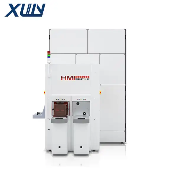
Used ASML HMI eScan 1100
Product Detail
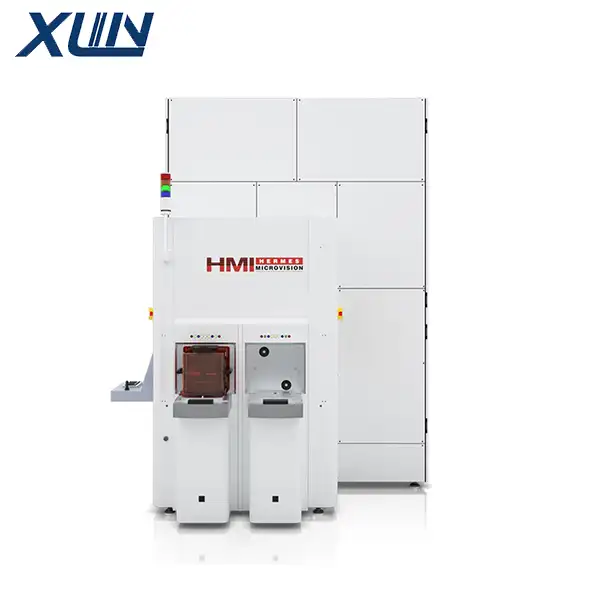 The HMI eScan 1100 is the first multi-electron-beam wafer inspection system from ASML designed for high-volume manufacturing (HVM) environments. It is primarily engineered to overcome the throughput bottlenecks associated with defect inspection in advanced process nodes.
Core Architecture and Performance
The system utilizes a 25-beam (5×5) multi-electron-beam architecture. Integrated with a high-speed wafer stage and a real-time computational framework, it delivers up to 15 times the throughput of single-beam inspection tools, meeting the in-line monitoring requirements for mass production at the 3nm node and beyond. Its advanced electron-optical system manages the 25 primary electron beams while suppressing inter-beam crosstalk, ensuring consistent imaging across all beams.
Inspection Capabilities
The system supports both voltage-contrast and physical defect inspection modes. It can detect electrical faults—such as open circuits, short circuits, and leakage—as well as physical pattern defects as small as 7nm. By leveraging a proprietary "Die-to-Database" function, the system achieves enhanced defect sensitivity and can be used to verify EUV reticle defects by inspecting their printed manifestations on wafers.
In short, the eScan 1100 transitions multi-electron-beam technology from R&D and validation into high-volume manufacturing, making high-resolution electron-beam inspection economically viable for production lines by providing sufficient wafer coverage.
Related Products
-
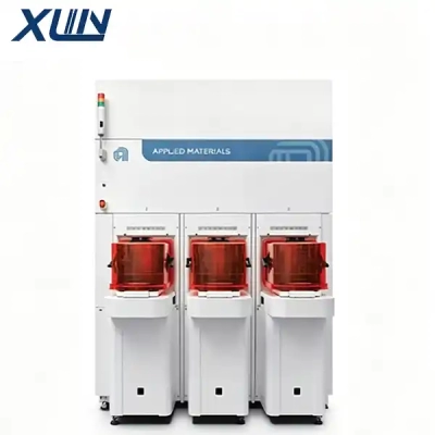
Applied Materials VeritySEM 6D CD-SEM for sale
-
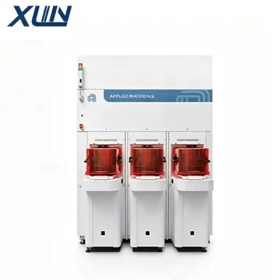
Used Applied Materials VeritySEM 6C CD-SEM
-
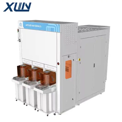
Applied Materials VeritySEM AP E-beam CD Metrology System
-
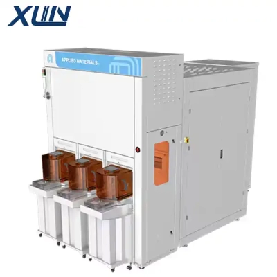
Applied Materials VeritySEM 20 CD-SEM for sale
-
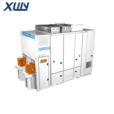
Applied Materials Vera Brightfield Patterned Wafer Optical Inspection System
-
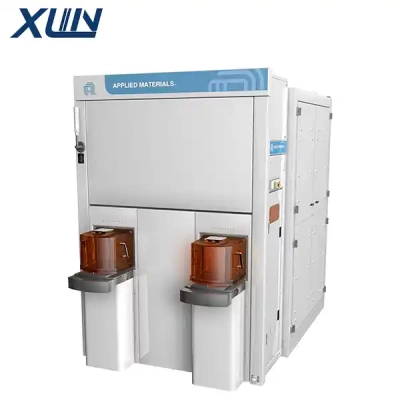
Used Applied Materials SEMVision H20