English
 南非荷兰语
 契维语
 阿姆哈拉语
 阿拉伯语
 阿萨姆语
 艾马拉语
 阿塞拜疆语
 白俄罗斯语
 保加利亚语
 孟加拉语
 波斯尼亚语
 加泰罗尼亚语
 宿务语
 科西嘉语
 捷克语
 威尔士语
 丹麦语
 de
 迪维希语
 希腊语
 英语
 爱沙尼亚语
 波斯语
 芬兰语
 爱尔兰语
 瓜拉尼语
 豪萨语
 希伯来语
 苗语
 克罗地亚语
 海地语
 匈牙利语
 亚美尼亚语
 印尼语
 冰岛语
 意大利语
 日语
 格鲁吉亚语
 高棉语
 韩语
 库尔德语
 吉尔吉斯语
 拉丁语
 卢森堡语
 卢干达语
 林加拉语
 老挝语
 立陶宛语
 拉脱维亚语
 毛利语
 马其顿语
 马来语
 马耳他语
 缅甸语
 尼泊尔语
 荷兰语
 挪威语
 齐切瓦语
 波兰语
 普什图语
 葡萄牙语
 罗马尼亚语
 俄语
 卢旺达语
 信德语
 僧伽罗语
 斯洛伐克语
 斯洛文尼亚语
 萨摩亚语
 索马里语
 阿尔巴尼亚语
 塞尔维亚语
 瑞典语
 斯瓦希里语
 塔吉克语
 泰语
 提格利尼亚语
 土库曼语
 土耳其语
 乌克兰语
 越南语
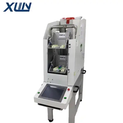
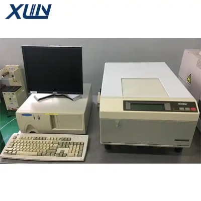
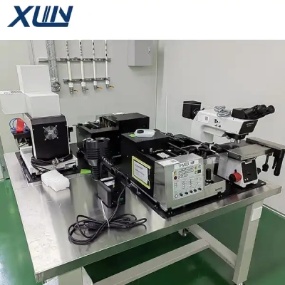
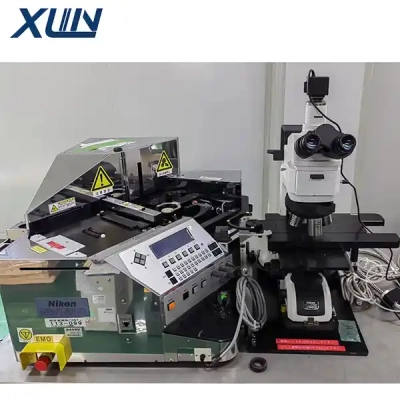
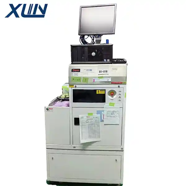
Used ECO 1000 FT-IR Infrared Spectroscopy Measurement System
Product Detail
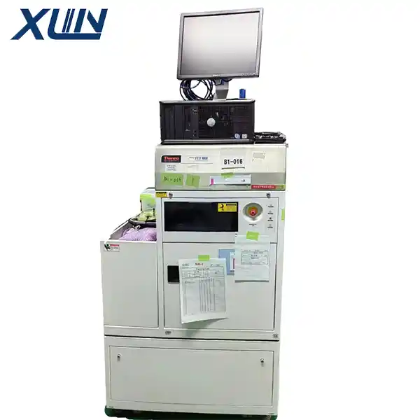 The ECO 1000 FT-IR is a fully automated Fourier-Transform Infrared (FT-IR) spectroscopy system designed specifically for semiconductor wafers (notably 200mm and 300mm). It is primarily used for measuring thin-film thickness and analyzing chemical composition in front-end-of-line (FEOL) processes and advanced packaging.
Core Focus: Non-Contact Thin-Film Metrology
By leveraging the interaction—specifically interference and absorption—between infrared light and the thin films on a wafer surface, the system performs non-destructive measurements of thickness and doping concentrations for epitaxial layers, dielectric films, photoresists, and SOI (Silicon-on-Insulator) structures. It is particularly well-suited for high-precision monitoring of film thickness uniformity on materials such as silicon and silicon carbide (SiC).
Key Technical Features
Broad Spectral Range and High-Precision Resolution: Covering a wide infrared spectrum, the system can accurately resolve the thickness of multi-layer film structures and ultra-thin epitaxial layers (e.g., SiC epitaxy), meeting the rigorous process requirements of compound semiconductors.
Fully Automated, High-Throughput Operation: Equipped with an automated wafer-handling system (compatible with FOUPs or open cassettes), the unit supports fully automated, multi-site measurements and the generation of wafer thickness maps. It also supports SECS/GEM communication protocols.
Non-Destructive and Cleanroom-Compatible: Utilizing optical, non-contact measurement techniques, the system eliminates the risk of scratches or particle contamination associated with physical probes, ensuring full compliance with the stringent cleanliness standards of semiconductor fabrication facilities (fabs).
Summary
With its high-precision, non-contact infrared measurement capabilities and fully automated, high-throughput design, the ECO 1000 FT-IR serves as a critical metrology tool for monitoring film thickness and ensuring yield in processes such as epitaxial growth, thin-film deposition, and the production of compound semiconductors (e.g., SiC).