English
 南非荷兰语
 契维语
 阿姆哈拉语
 阿拉伯语
 阿萨姆语
 艾马拉语
 阿塞拜疆语
 白俄罗斯语
 保加利亚语
 孟加拉语
 波斯尼亚语
 加泰罗尼亚语
 宿务语
 科西嘉语
 捷克语
 威尔士语
 丹麦语
 de
 迪维希语
 希腊语
 英语
 爱沙尼亚语
 波斯语
 芬兰语
 爱尔兰语
 瓜拉尼语
 豪萨语
 希伯来语
 苗语
 克罗地亚语
 海地语
 匈牙利语
 亚美尼亚语
 印尼语
 冰岛语
 意大利语
 日语
 格鲁吉亚语
 高棉语
 韩语
 库尔德语
 吉尔吉斯语
 拉丁语
 卢森堡语
 卢干达语
 林加拉语
 老挝语
 立陶宛语
 拉脱维亚语
 毛利语
 马其顿语
 马来语
 马耳他语
 缅甸语
 尼泊尔语
 荷兰语
 挪威语
 齐切瓦语
 波兰语
 普什图语
 葡萄牙语
 罗马尼亚语
 俄语
 卢旺达语
 信德语
 僧伽罗语
 斯洛伐克语
 斯洛文尼亚语
 萨摩亚语
 索马里语
 阿尔巴尼亚语
 塞尔维亚语
 瑞典语
 斯瓦希里语
 塔吉克语
 泰语
 提格利尼亚语
 土库曼语
 土耳其语
 乌克兰语
 越南语
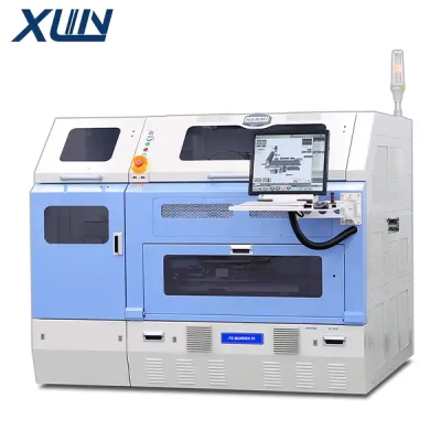
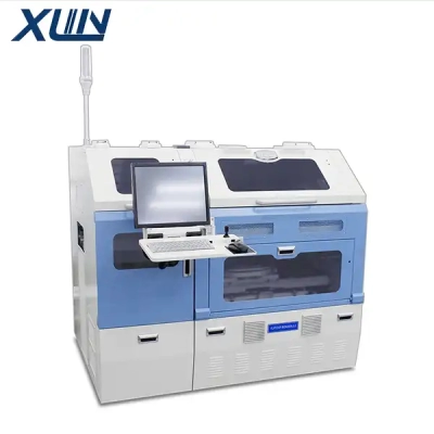
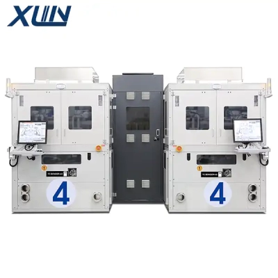
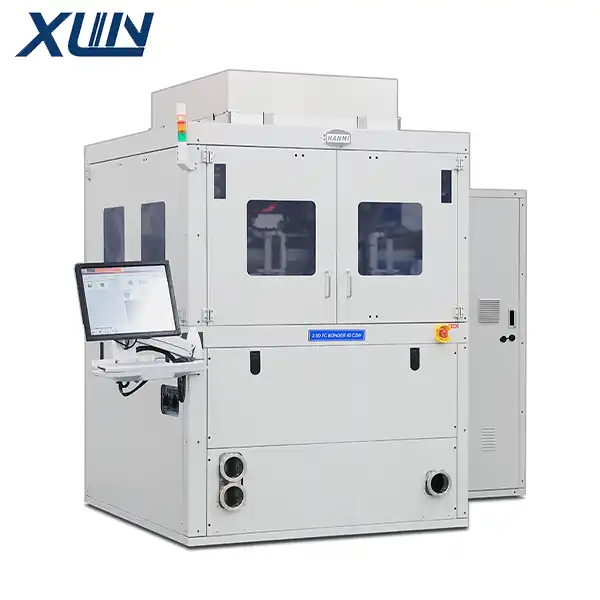
HANMI 2.5D TC BONDER 40 C2W TCB die bonder
Product Detail
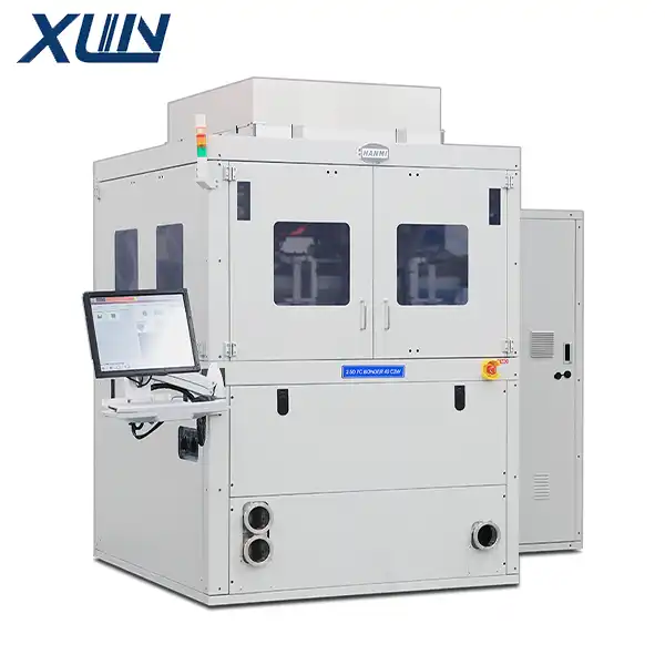 The HANMI 2.5D TC Bonder 40 C2W is a thermal compression (TC) bonding system designed specifically for high-performance 2.5D semiconductor packaging. Its primary function is the high-precision bonding of individual chips onto a wafer.
Core Positioning
Developed by HANMI Semiconductor, this system is part of a product line tailored for 2.5D packaging of AI system semiconductors. The "C2W" designation stands for "Chip-to-Wafer"—a process involving the bonding of singulated chips onto a full wafer—which distinguishes it from "C2S" (Chip-to-Substrate) processes.
Key Capabilities
According to official product specifications, the system is engineered for the precision bonding of chips, supporting dimensions up to 40mm × 40mm. It is designed for 2.5D advanced packaging applications essential for AI hardware, such as integrating various components—including GPUs, CPUs, or HBM (High Bandwidth Memory)—onto a single package via a silicon interposer. Deliveries of this model to global foundry and OSAT (Outsourced Semiconductor Assembly and Test) customers for mass production began in late 2025.
Summary
This is a high-precision 2.5D packaging tool that utilizes thermal compression to bond chips onto wafers, specifically targeting the "Chip-to-Wafer" process stage for AI system semiconductors.