English
 南非荷兰语
 契维语
 阿姆哈拉语
 阿拉伯语
 阿萨姆语
 艾马拉语
 阿塞拜疆语
 白俄罗斯语
 保加利亚语
 孟加拉语
 波斯尼亚语
 加泰罗尼亚语
 宿务语
 科西嘉语
 捷克语
 威尔士语
 丹麦语
 de
 迪维希语
 希腊语
 英语
 爱沙尼亚语
 波斯语
 芬兰语
 爱尔兰语
 瓜拉尼语
 豪萨语
 希伯来语
 苗语
 克罗地亚语
 海地语
 匈牙利语
 亚美尼亚语
 印尼语
 冰岛语
 意大利语
 日语
 格鲁吉亚语
 高棉语
 韩语
 库尔德语
 吉尔吉斯语
 拉丁语
 卢森堡语
 卢干达语
 林加拉语
 老挝语
 立陶宛语
 拉脱维亚语
 毛利语
 马其顿语
 马来语
 马耳他语
 缅甸语
 尼泊尔语
 荷兰语
 挪威语
 齐切瓦语
 波兰语
 普什图语
 葡萄牙语
 罗马尼亚语
 俄语
 卢旺达语
 信德语
 僧伽罗语
 斯洛伐克语
 斯洛文尼亚语
 萨摩亚语
 索马里语
 阿尔巴尼亚语
 塞尔维亚语
 瑞典语
 斯瓦希里语
 塔吉克语
 泰语
 提格利尼亚语
 土库曼语
 土耳其语
 乌克兰语
 越南语
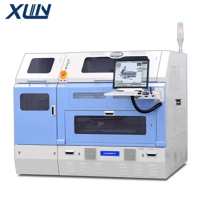
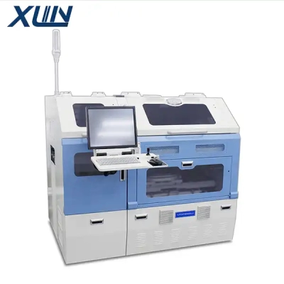
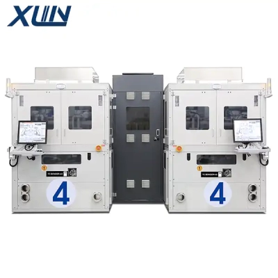
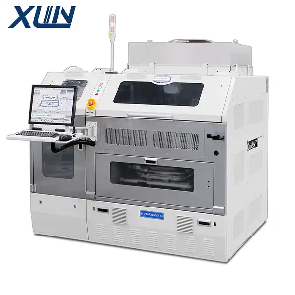
HANMI FC Bonder 3.5 Flip-Chip Bonder for sale
Product Detail
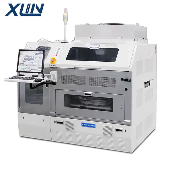 The HANMI FC Bonder 3.5 is a high-end flip-chip bonder introduced by HANMI Semiconductor in June 2026, designed for 2.5D packaging of AI system semiconductors. This launch marks a strategic expansion for the company, moving beyond its established position in TC bonders for HBM (High Bandwidth Memory) into the broader field of system semiconductor packaging equipment.
Core Positioning and Process Capabilities
Specifically engineered for 2.5D logic chip packaging, the system supports Chip-to-Wafer (C2W) bonding and can accommodate large-format panels and substrates up to 340mm. This capability directly addresses the industry trend toward Panel-Level Packaging (PLP) and multi-chip (chiplet) architectures for AI processors. In addition to flip-chip bonding, the equipment supports "face-up" (non-flip-chip) bonding using Die Attach Film (DAF), offering customers greater process flexibility.
Market Significance
Following the release of the FC Bonder 75 in 2025, the FC Bonder 3.5 represents another key move by HANMI Semiconductor into the system semiconductor packaging sector. The equipment targets global wafer foundries and OSAT (Outsourced Semiconductor Assembly and Test) providers, serving major AI chip developers—such as NVIDIA, AMD, and Broadcom—that utilize 2.5D packaging technologies. According to HANMI, the system leverages the company’s proven bonding expertise—honed through its HBM TC bonder technology—with the goal of extending its competitive edge from memory packaging into the back-end processing of system semiconductors.