English
 南非荷兰语
 契维语
 阿姆哈拉语
 阿拉伯语
 阿萨姆语
 艾马拉语
 阿塞拜疆语
 白俄罗斯语
 保加利亚语
 孟加拉语
 波斯尼亚语
 加泰罗尼亚语
 宿务语
 科西嘉语
 捷克语
 威尔士语
 丹麦语
 de
 迪维希语
 希腊语
 英语
 爱沙尼亚语
 波斯语
 芬兰语
 爱尔兰语
 瓜拉尼语
 豪萨语
 希伯来语
 苗语
 克罗地亚语
 海地语
 匈牙利语
 亚美尼亚语
 印尼语
 冰岛语
 意大利语
 日语
 格鲁吉亚语
 高棉语
 韩语
 库尔德语
 吉尔吉斯语
 拉丁语
 卢森堡语
 卢干达语
 林加拉语
 老挝语
 立陶宛语
 拉脱维亚语
 毛利语
 马其顿语
 马来语
 马耳他语
 缅甸语
 尼泊尔语
 荷兰语
 挪威语
 齐切瓦语
 波兰语
 普什图语
 葡萄牙语
 罗马尼亚语
 俄语
 卢旺达语
 信德语
 僧伽罗语
 斯洛伐克语
 斯洛文尼亚语
 萨摩亚语
 索马里语
 阿尔巴尼亚语
 塞尔维亚语
 瑞典语
 斯瓦希里语
 塔吉克语
 泰语
 提格利尼亚语
 土库曼语
 土耳其语
 乌克兰语
 越南语
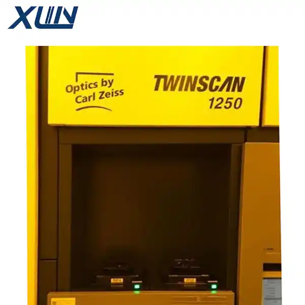
Used ASML XT:1250i for sale
Product Detail
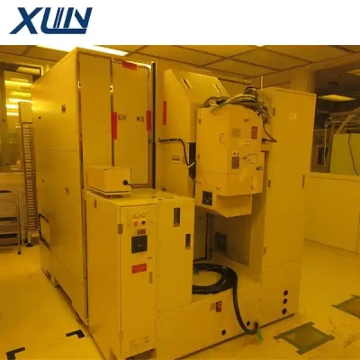
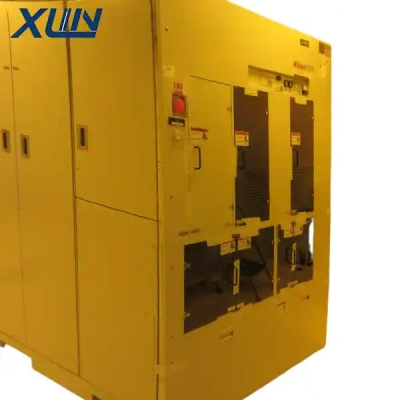
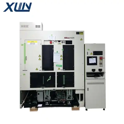
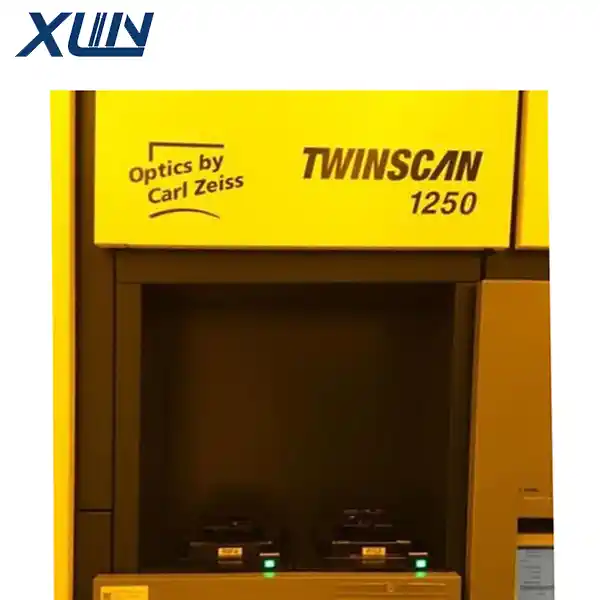 The ASML XT:1250i is a fully automated step-and-scan lithography system (scanner) designed for 300mm (12-inch) wafers. Part of ASML’s classic XT platform, it utilizes an i-line (365nm) light source.
Core Positioning: A Workhorse for Advanced Packaging and Thick-Resist Processes
This system primarily serves mature process nodes (0.35μm and above), but it excels particularly in advanced packaging—such as Flip-Chip, Fan-Out, and 2.5D/3D integration—as well as in MEMS manufacturing. The i-line light source offers excellent penetration depth in thick photoresists, making the system a critical tool for patterning steps in packaging production lines.
Key Technical Features
Large Exposure Field and High Depth of Focus: Equipped with an i-line lens that provides a deep depth of focus, the system is ideally suited for thick-resist processes (e.g., creating bumps tens of microns high or forming redistribution layers). Its step-and-scan architecture ensures high pattern fidelity across the entire exposure field.
Superior Handling of Warped Wafers: To address wafer warpage and surface topography variations—common challenges in advanced packaging—the system features optimized leveling and alignment subsystems, ensuring high-precision overlay accuracy even on non-planar surfaces.
High Throughput and Automation: The system comes standard with a fully automated 300mm wafer handling system (FOUP) and delivers high throughput. It supports SECS/GEM communication, allowing for seamless integration into automated high-volume production lines. The XT platform is mature, stable, and offers a lower cost of ownership.
Summary
With its unique advantages in thick-resist processing (leveraging an i-line light source), exceptional capability in handling warped wafers, and high throughput, the XT:1250i serves as an indispensable core lithography tool for 300mm advanced packaging and mature-node semiconductor manufacturing.