English
 南非荷兰语
 契维语
 阿姆哈拉语
 阿拉伯语
 阿萨姆语
 艾马拉语
 阿塞拜疆语
 白俄罗斯语
 保加利亚语
 孟加拉语
 波斯尼亚语
 加泰罗尼亚语
 宿务语
 科西嘉语
 捷克语
 威尔士语
 丹麦语
 de
 迪维希语
 希腊语
 英语
 爱沙尼亚语
 波斯语
 芬兰语
 爱尔兰语
 瓜拉尼语
 豪萨语
 希伯来语
 苗语
 克罗地亚语
 海地语
 匈牙利语
 亚美尼亚语
 印尼语
 冰岛语
 意大利语
 日语
 格鲁吉亚语
 高棉语
 韩语
 库尔德语
 吉尔吉斯语
 拉丁语
 卢森堡语
 卢干达语
 林加拉语
 老挝语
 立陶宛语
 拉脱维亚语
 毛利语
 马其顿语
 马来语
 马耳他语
 缅甸语
 尼泊尔语
 荷兰语
 挪威语
 齐切瓦语
 波兰语
 普什图语
 葡萄牙语
 罗马尼亚语
 俄语
 卢旺达语
 信德语
 僧伽罗语
 斯洛伐克语
 斯洛文尼亚语
 萨摩亚语
 索马里语
 阿尔巴尼亚语
 塞尔维亚语
 瑞典语
 斯瓦希里语
 塔吉克语
 泰语
 提格利尼亚语
 土库曼语
 土耳其语
 乌克兰语
 越南语
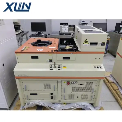
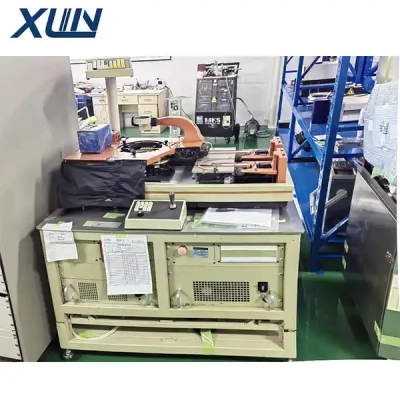
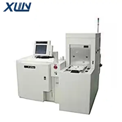
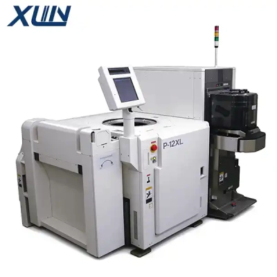
Used TEL Probe Station Cellcia™
Product Detail
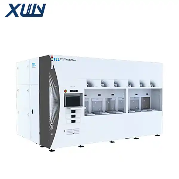
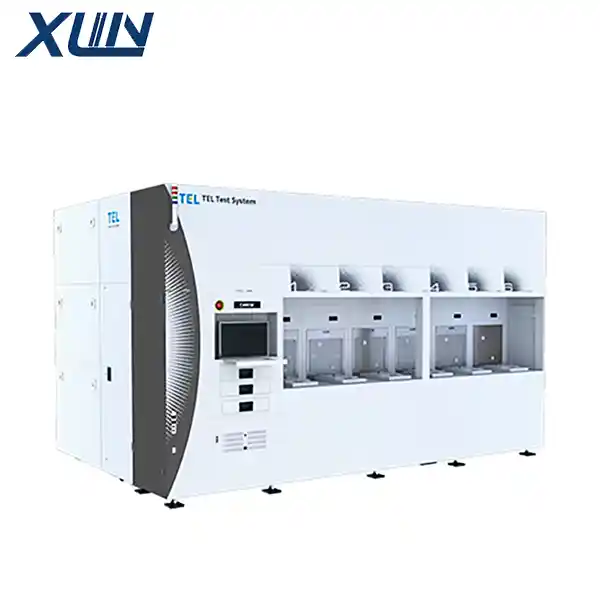 TEL Cellcia™ is not a conventional wafer prober; rather, it is a multi-unit parallel testing platform designed for 300mm wafers. Moving beyond the traditional approach of simply increasing the speed of an individual prober, Cellcia utilizes multiple independent test units that operate concurrently to reduce the total turnaround time for an entire batch of wafers.
Architecture and Throughput Logic
The most distinctive feature of Cellcia is its multi-section, multi-layer architecture. The system can be configured with 12 or 25 independent test units, each capable of processing wafers simultaneously. By distributing a batch of wafers across these units for parallel testing, the time required to complete the entire batch is significantly shortened. This stacked, multi-layer design also drastically reduces the equipment's footprint, resulting in a much higher throughput per unit area compared to traditional wafer probers.
Core Specifications
The system supports 300mm wafers, features an XY probing accuracy of ±5.0 μm, and supports a maximum probing force of 200 kg. It employs a vacuum-contact chuck, utilizes an ASU/BCU-II optical system, and runs on an operating system based on Windows and PLC. Its primary applications include memory testing and wafer-level burn-in.
In short, Cellcia is a 300mm memory wafer testing platform that leverages a parallel architecture to boost throughput. Its value lies not in pushing the limits of single-point precision, but in minimizing the total test time for an entire batch through the simultaneous operation of multiple test units.