English
 南非荷兰语
 契维语
 阿姆哈拉语
 阿拉伯语
 阿萨姆语
 艾马拉语
 阿塞拜疆语
 白俄罗斯语
 保加利亚语
 孟加拉语
 波斯尼亚语
 加泰罗尼亚语
 宿务语
 科西嘉语
 捷克语
 威尔士语
 丹麦语
 de
 迪维希语
 希腊语
 英语
 爱沙尼亚语
 波斯语
 芬兰语
 爱尔兰语
 瓜拉尼语
 豪萨语
 希伯来语
 苗语
 克罗地亚语
 海地语
 匈牙利语
 亚美尼亚语
 印尼语
 冰岛语
 意大利语
 日语
 格鲁吉亚语
 高棉语
 韩语
 库尔德语
 吉尔吉斯语
 拉丁语
 卢森堡语
 卢干达语
 林加拉语
 老挝语
 立陶宛语
 拉脱维亚语
 毛利语
 马其顿语
 马来语
 马耳他语
 缅甸语
 尼泊尔语
 荷兰语
 挪威语
 齐切瓦语
 波兰语
 普什图语
 葡萄牙语
 罗马尼亚语
 俄语
 卢旺达语
 信德语
 僧伽罗语
 斯洛伐克语
 斯洛文尼亚语
 萨摩亚语
 索马里语
 阿尔巴尼亚语
 塞尔维亚语
 瑞典语
 斯瓦希里语
 塔吉克语
 泰语
 提格利尼亚语
 土库曼语
 土耳其语
 乌克兰语
 越南语
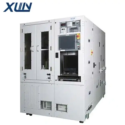
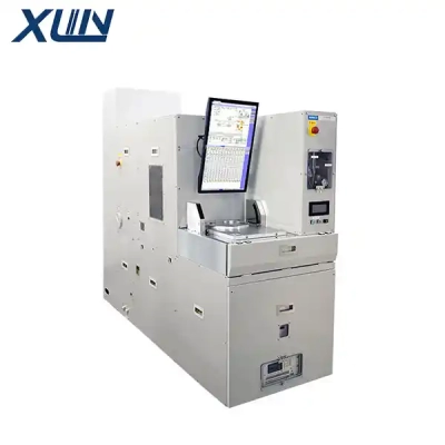
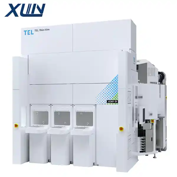
Used TEL Thin Flim Deposition Equipment LEXIA™-EX
Product Detail
 The TEL LEXIA™-EX is a single-wafer dielectric thin-film deposition platform from Tokyo Electron (TEL) designed for 300mm advanced logic and memory chip manufacturing; it represents the latest generation in the LEXIA series. Rather than being an ALD (Atomic Layer Deposition) system, it utilizes CVD/PECVD (Chemical Vapor Deposition/Plasma-Enhanced CVD) processes to deposit dielectric films, positioning it as a competitor to single-wafer PECVD tools such as the Novellus Vector Express.
Process Positioning: The LEXIA-EX is primarily tasked with dielectric thin-film deposition at advanced nodes. Typical applications include sidewall spacers, etch-stop layers, diffusion barriers, hard masks, and films used for planarization. The system supports a wide range of precursor chemistries, enabling the deposition of silicon oxide, silicon nitride, and doped dielectric films, with process recipes that can be flexibly adapted to various integration schemes. Its single-wafer architecture ensures excellent within-wafer uniformity and wafer-to-wafer repeatability, meeting the stringent requirements for film thickness and interface quality demanded by advanced logic devices.
Platform Design: Built on TEL’s 300mm cluster platform, the system can integrate multiple process modules to meet high-volume manufacturing throughput requirements. The reaction chambers are optimized for thermal budget control and particle suppression; combined with precise gas delivery and temperature control systems, they ensure high film density while minimizing defect density. Within TEL’s deposition portfolio, the LEXIA series serves as the primary workhorse for high-volume dielectric film deposition, complementing the EVAROS and EXIM systems—which focus on ALD—by addressing a different segment of the process technology spectrum.
Applications: The LEXIA-EX is primarily used in the patterning and interconnect modules of advanced logic chips, and it can also be applied to the deposition of dielectric layers in memory devices. While its application scope overlaps in certain areas with ASM’s XP8 Synergis thermal ALD platform and XP8 PEALD series, its technical approach is centered on CVD rather than atomic-layer-level deposition.
In short, the LEXIA-EX is TEL’s primary high-volume production platform for single-wafer dielectric CVD at advanced nodes. Together with the ALD/PEALD equipment you have previously looked into, it completes the full picture of advanced thin-film deposition processes.